1,Hight prurity (99.99% min) Metal Antimony (Sb) 2,4N>99.99%, 5N>99.999%, 6N>99.9999%, 7N>99.99999% 3,Lumps/Ingot/Granule/Bar 4,Color: Gray 5,Atomic weight: 121.760 6,Electronegativity: 2.05 7,CAS No.: 7440-36-0 8,Density: 6.697 g/cm3 (25â??) 9,Melting Point: 630.63 â?? 10,Boiling Point: 1587 â?? 11,Mainly used for the preparation of â?¢ - V compound semiconductor InSb, Bi2Sb, GaSb, high purity alloys, electronic refrigeration element materials and germanium, silicon single crystal dopants.

The UV laser marking machine is developed by using a 355nm UV laser. This machine uses a third-order intracavity frequency doubling technology. Compared with infrared lasers, the 355nm UV laser has a very small spot, and the marking effect is directly interrupted by a short-wavelength laser. The molecular chain greatly reduces the mechanical deformation of the material. Thermal deformation (cold light), because it is mainly used for ultra-fine marking and engraving. It is especially suitable for applications such as marking, micro-hole drilling of food and pharmaceutical packaging materials, high-speed dicing of glass materials, and complex pattern cutting of silicon wafers.
Size: 19*11cm Necklace size:25cm Weight:90g Infant baby kid washable silicone feeding bib 100% brand new and high quality Can be safely washed in the dishwasher or wiped clean Roll up bib for easy travel and storage Has a built in crumb catcher and adjustable clasp For use on babies 6 months and older All products have been tested for safety These silicone bibs do not contain lead, bpa, phthalates, latex, or pvc
Place of origin united states Brand name bondatek Bondatek provides ge, gaas, gap, gan, gasb, inp, inas, insb wafers to micro- electronics and optoelectronics industry in diameter range from 2" to 4" with orientation or , epd< 5000 cm-2 and epi ready surface. Inp based 25 piece/pieces
Advantage of top quality factory price 156x156mm 200um high quality Hot Sales A Grade polysilicon wafer The production process is simple, cost-effective, and reduces silicon waste High conversion efficiency, low fragmentation rate and low optical attenuation Manufacturing Specialization, Intelligence and Greening Customized products to meet customer needs Technology : Diamond wire cutting Type : P type Resistance:1~3μs minority carrier:>2 μs Hem width:157.00~157.25mm Thickness:200±20μm Transfer efficiency:>18.8%
Advantage of top quality factory price 156x156mm 200um high quality Hot Sales A Grade polysilicon wafer ?The production process is simple, cost-effective, and reduces silicon waste ?High conversion efficiency, low fragmentation rate and low optical attenuation ?Manufacturing Specialization, Intelligence and Greening ?Customized products to meet customer
Name: High efficiency polysilicon wafer Technology : Diamond wire cutting Type : P type Resistance:1~3 minority carrier:>2 Hem width:157.00~157.25mm Thickness:200±20 m Transfer efficiency:>18.8% Advantage of top quality factory price 156x156mm 200um high quality Hot Sales A Grade polysilicon wafer The production process is simple, cost-effective, and reduces silicon waste High conversion efficiency, low fragmentation rate and low optical attenuation Manufacturing Specialization, Intelligence and Greening Customized products to meet customer needs
Name: High efficiency polycrystalline silicon block Technology :Semi-melting Type: P Type Resistance:1~3©cm minority carrier :>6s Hem width:157.00~157.25mm Angle of Chamfer:1~2mm Name: High efficiency polysilicon wafer Technology : Diamond wire cutting Type : P type Resistance:1~3s minority carrier:>2 s Hem width:157.00~157.25mm Thickness:200±20m Transfer efficiency:>18.8%
Name: High efficiency polycrystalline silicon block Technology :Semi-melting Type: P Type Resistance:1~3©cm minority carrier :>6s Hem width:157.00~157.25mm Angle of Chamfer:1~2mm Name: High efficiency polysilicon wafer Technology : Diamond wire cutting Type : P type Resistance:1~3s minority carrier:>2 s Hem width:157.00~157.25mm Thickness:200±20m Transfer efficiency:>18.8%
Name: High efficiency polysilicon wafer Technology : Diamond wire cutting Type : P type Resistance:1~3s minority carrier:>2 s Hem width:157.00~157.25mm Thickness:200±20m Transfer efficiency:>18.8% Name: High efficiency polycrystalline silicon block Technology :Semi-melting Type: P Type Resistance:1~3©cm minority carrier :>6s Hem width:157.00~157.25mm Angle of Chamfer:1~2mm
Advantage of top quality factory price 156x156mm 200um high quality Hot Sales A Grade polysilicon wafer Manufacturer The production process is simple, cost-effective, and reduces silicon waste High conversion efficiency, low fragmentation rate and low optical attenuation Manufacturing Specialization, Intelligence and Greening Customized products to meet customer needs Name: High efficiency polysilicon wafer Technology : Diamond wire cutting Type : P type Resistance:1~3s minority carrier:>2 s Hem width:157.00~157.25mm Thickness:200±20m Transfer efficiency:>18.8%
Advantage of Hot Sales A Grade polysilicon wafer The production process is simple, cost-effective, and reduces silicon waste High conversion efficiency, low fragmentation rate and low optical attenuation Manufacturing Specialization, Intelligence and Greening Customized products to meet customer needs Name: High efficiency polysilicon wafer Technology : Diamond wire cutting Type : P type Resistance:1~3s minority carrier:>2 s Hem width:157.00~157.25mm Thickness:200±20m Transfer efficiency:>18.8% http://en.hengxingchinese.com/ Hengxing company website: https://hengxingsteelwire.com/ Email contact US:wmsale@hxkjgf.com
Advantage of P Type Polycrystalline Solar Wafer Manufacturer The production process is simple, cost-effective, and reduces silicon waste High conversion efficiency, low fragmentation rate and low optical attenuation Manufacturing Specialization, Intelligence and Greening Customized products to meet customer needs Technology : Diamond wire cutting Type : P type Resistance:1~3 s minority carrier:>2 s Hem width:157.00~157.25mm Thickness:200±20m Transfer efficiency:>18.8%
Technology : Diamond wire cutting Type : P type Resistance:1~3s minority carrier:>2 s Hem width:157.00~157.25mm Thickness:200±20m Transfer efficiency:>18.8% Advantage of high quality Hot Sales A Grade polysilicon wafer The production process is simple, cost-effective, and reduces silicon waste High conversion efficiency, low fragmentation rate and low optical attenuation Manufacturing Specialization, Intelligence and Greening Customized products to meet customer needs
Advantage of High efficiency P Type polysilicon wafer The production process is simple, cost-effective, and reduces silicon waste High conversion efficiency, low fragmentation rate and low optical attenuation Manufacturing Specialization, Intelligence and Greening Customized products to meet customer needs Technology : Diamond wire cutting Type : P type Resistance:1~3s minority carrier:>2 s Hem width:157.00~157.25mm Thickness:200±20m Transfer efficiency:>18.8%
Advantage of Hot Sales A Grade polysilicon wafer The production process is simple, cost-effective, and reduces silicon waste High conversion efficiency, low fragmentation rate and low optical attenuation Manufacturing Specialization, Intelligence and Greening Customized products to meet customer needs Technology : Diamond wire cutting Type : P type Resistance:1~3s minority carrier:>2 s Hem width:157.00~157.25mm Thickness:200±20m Transfer efficiency:>18.8%
Technology : Diamond wire cutting Type : P type Resistance:1~3μs minority carrier:>2 μs Hem width:157.00~157.25mm Thickness:200±20μm Transfer efficiency:>18.8% Hengxing science and techology co.,ltd built in 1995, with 24 years of steel wire transforming and coating industries, our main product as galavanized steel wire, strand, PC steel wire strand, steel cord radial tire, hyrolic hose and polycrystaline silicon. Listed on Shenzhen A stock market in 2007,we have independent R&D center, passed the ISO, SGS,BV certification and so on. As the biggest galavanized steel wire and srand manufacture in China, and the biggest steel cord for radial tire, with high quality and performance, our product widely used in the industries as electric cable, suspension construction, radial tire and hydrolic hose, and sawing.
Advantage of high quality P Type Polycrystalline Solar Wafer The production process is simple, cost-effective, and reduces silicon waste High conversion efficiency, low fragmentation rate and low optical attenuation Manufacturing Specialization, Intelligence and Greening Customized products to meet customer needs Technology : Diamond wire cutting Type : P type Resistance:1~3 s minority carrier:>2 s Hem width:157.00~157.25mm Thickness:200±20 m Transfer efficiency:>18.8%
CVD Diamond has been recognized an ideal material for various applications because of its outstanding properties which includes extreme hardness and strength, high thermal conductivity, low thermal expansion, excellent dielectric properties, resistance to chemical attack, and optical transmission over a wide spectral range. It can be widely used in complex tooling and machining processes, thermal-management applications, semiconductor industry and microwave engineering. Microwave-Transparent Windows and Optics We supply high-quality diamond optical products that are transparent in the microwave region with a wide range of size and thickness. With our cutting-edge laser technologies, we can customize the optical windows in any shape and dimension according to clients requirement. Specifications: Diameter of 65mm (F150mm on request) Double side surface roughness: Ra 10nm Flatness: 4um/cm With higher transparency Thickness less than 0.5mm Can be laser cut to any size and shapes
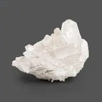
Quartz, the main component of glass, has a variety of different applications in various industries such as construction granulates and solar panels. It's a hard, crystalline mineral made up of silicon and oxygen atoms, and it's also the second most widely available mineral in the earth's crust after the feldspar Quartz mineral has hexagonal-shaped crystals. The color range for quartz is massive. This adaptable mineral is both long-lasting and chemically inert, with high heat resistance and electrical qualities. We source the majority of our quartz minerals from the regions of Rajasthan, Bihar and Andhra Pradesh. It is an extremely useful mineral in the manufacturing of solar panels, semiconductors and electronics, aluminium and steel alloys, and also in the construction sector, after being transformed into silicon (Si) through gaseous reduction at high temperatures. The physical properties of the quartz mineral are chemical inertness, thermal stability and electrical properties. It is also known for its hardness and it ranks 7 on the Mohs scale. Our high-purity quartz mineral finds its usage in the manufacturing of the casting of silicon for photovoltaic cells that make up solar panels and semiconductor components. Quartz is a hard, crystalline mineral composed of silica (silicon dioxide). The atoms are linked in a continuous framework of SiO4 silicon-oxygen tetrahedra, with each oxygen being shared between two tetrahedra, giving an overall chemical formula of SiO2. Within the sector of aluminium and iron & steel industries, quartz pebbles once converted to silicon, are critical components in the production of ferro-alloys and silicon for aluminium alloys and silicone. Further, in the refractories, high-grade quartzite-based silica minerals have been used in the fabrication of linings for the coreless induction furnaces for melting and retaining iron for decades. We at Aryan Tiles will keep its development efforts focused on developing new markets for its high-purity quartz products that promote the usage of renewable energy sources like solar power cells.