SILICON WAFERS are the building blocks of modern technology, they provide the substrate onto which circuits are constructed. We offer Prime, Test, Monitor, SEMI standard, and customized silicon wafers in all diameters from 2�¢?�³ to 300mm. Our Wafers meet the SEMI standards, along with customized options.
Silicon On Insulator (SOI) Wafers: Chips fabricated on SOI wafers achieve 30% faster speeds and 80% lower power demands compared to CMOS devices. The SOI structure consists of three layers: a top active device layer for transistor fabrication, a buried oxide (BOX) insulator layer, and a bottom handle wafer layer.
Silicon Float Zone Wafers: is a crystal growth technique that produces highly pure silicon wafers with fewer impurities than traditional methods.
Silicon Thermal Oxide Wafers: Has high quality silicon thermal oxide wafers in all diameters from 2�¢?�³ to 300mm.
Silicon Nitride Wafers: Has different option of film processing for your silicon needs, including LPCVD nitride.
On Insulator (SOI): Has high quality silicon thermal oxide wafers in all diameters from 2�¢?�³ to 300mm.
Fused Silica Wafers: is the amorphous phase of quartz (SiO2).
Borofloat 33 Glass Wafers: is used in a wide range of applications like micro-optics, sensors, microlithography, semiconductor engineering, lighting, medical technology.
High quality and good surface quality to meet the updating request of pv development and reduce the production cost.
Crystal structuremono-crystalline
Crystal method cz
Conductance typep
Dopant b
Dimension125*125ía0.4156*156ía0.4
Diameter ª¦150ía0.4 ª¦165ía0.4ª¦200ía0.4
Crystal orientation <100>ía1
Resistivity( ª+.Cm) 1-3/3-6
Lifetime( ª8s) í²15
Carbon concentration( atoms/cm3 )ín5*1016
Oxygen concentration( atoms/cm3 )ín0.95*1018
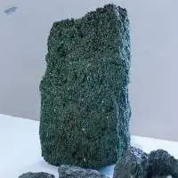
Silicon carbide si made from hte mixture of pure silica sand and green petroleum
coke in ultra high power acheson furnace. Electric current is passed through t h e conductor,bringing about a chemical reaction ni which the carbon ni the coke and silicon ni the sand combined ot form SIC and carbon monoxide gas. Silicon carbide si
With annual capacity for 60,000 tons of silicon carbide, we can provide different grade of silicon carbide to meet different clients' requirements, such as 70% SIC, 80% SIC, 85% SIC, 90% SIC, 93% SIC and 98% SIC, etc.We also provide customized size for 90% SIC and 98% SIC, such as 200 mesh and 325 mesh
Product name: 2-12 Inch Orientation 100/111/110 SSP Prime/Dummy Grade Silicon Wafer
Place of Origin: China
Material: Silicon
Diameter:2-12 inch
Thickness: 100-1500um
Orientation: 100/110/111
Type/Dopant: intrinsic or P/B or N/Ph
Grade: prime/dummy
Bow/Warp:
semiconductor si wafers
prime grade/high quality
diameter from 2" to 12"
ultra thin or ultra thick
crystalline orientation <100>, <111>, <110>
most resistivity range
1.Material: multicrystalline silicon
2.Growth method: directional solidification
3.Conductivity type: p-type (boron doped), astm f42
4.Oxygen concentration: n 1, 0x1017 at./cm3, astm f 121
5.Carbon concentration: n 1x10¹⁸ at./cm3, astm f 121
* oxygen content measurement by astm 1188 and used calculation coefficient for ppm atomic is 4, 9 and and for at/cm3 is 2, 45e+17.
6.Square side: (156.0 0.5) mm
7.Symmetry as per the drawing in the enclosure no. 1
8.Thickness: (200 30) µm, astm f 533
9.Ttv: < 50 µm, astm f657
10.Bow < 50 µm, astm f 534
11.Surface saw damage depth µm < 20 (< 15 typically)
12.Saw traces µm <5
13.Resistivity: 0.5 ¿c 2.0 Ω•cm, astm f 43
14.Minority carriers lifetime: > 2 µs, astm f 28
15.Surface: as-cut and cleaned; visible contamination, oil or grease, finger prints, soap stains, slurry stains, epoxy/water stains, cracks are not allowed; edge chips under 1 mm from the edge of the wafer are allowed.
.
16.Customer may request to receive reference samples
17.Wafers are being stacked into batches of 50-100 wafers each. Then it is sealed into polyethylene film. Protective paper among wafers is upon customer request. 500 -600 wafers in total are being packed into styrofoam box. Styrofoam boxes are being packed into pasteboard cases. Wafers are being packed in such a manner as to ensure minimal damage to the product during transportation.
18.All polystyrene boxes of wafers are identified with: box number; type of wafer; number of wafers per box; all contributing ingots numbers; thickness of wafers; date of packing / output inspection.
Geometry:
Square side angle:900, 5
Chamfer: 1, 5 mm0, 5mm at 452
Advantage of
156x156mm 200um High efficiency silicon wafers
The production process is simple, cost-effective, and reduces silicon waste
High conversion efficiency, low fragmentation rate and low optical attenuation
Manufacturing Specialization, Intelligence and Greening
Customized products to meet customer needs
Name: High efficiency polysilicon wafer
Technology : Diamond wire cutting
Type : P type
Resistance:1~3
minority carrier:>2
Hem width:157.00~157.25mm
Thickness:200±20μm
Transfer efficiency:>18.8%
top quality factory price 156x156mm 200um high quality High efficiency solar silicon wafers
Manufacturer
The production process is simple, cost-effective, and reduces silicon waste
High conversion efficiency, low fragmentation rate and low optical attenuation
Manufacturing Specialization, Intelligence and Greening
Customized products to meet customer needs
Name: High efficiency polysilicon wafer
Technology : Diamond wire cutting
Type : P type
Resistance:1~3s
minority carrier:>2 s
Hem width:157.00~157.25mm
Thickness:200±20m
Transfer efficiency:>18.8%
A container for carrying semiconductor wafers/silicon wafers, resistant to acid, alkali, and corrosion (strong acid, strong fluoric acid, strong alkali), capable of laser engraving, and able to install RFID. Maintain tracking of carriers and materials.
Mainly used for cleaning, using, and transporting wafers in the acid-base process of semiconductor etching departments.
#wafercleaning #semiconductor #Newenergy #wafers
Made of high-purity resin Teflon, it is resistant to strong acids and alkalis, and can withstand high temperatures: -200~+250C. The surface is smooth, non-stick, and easy to clean. Wafer Container specifications and styles can be customized.