Button Cu Plating manufacturing specification [FPCB D/S] 1. Layer : Double side FPCB + Partial PSR 2. Application : Sensor 3. Thickness : CON. 0.2 T 4. L/S : 125 micrometer/125 micrometer 5. Laser drill : 50 micrometer 6. Copper plating : Hole inner Min. 25 micrometer 7.Inspection spec :Not allowing damage on copper plating part 8. SPECIAL item for controlling : - Stair-shape at Copper plating neighboring area - Apply WET LAMINATION method
1. Good quality and best price 2. No MOQ 3. UL, CE, ISO900, TS16949 4. ROSH Flexible printed circuit board, FPC, FPCB board We are specialized in producing FPC (Flexible PCB), PCB, PCBA factory. 1. Single sided FPCB: One single conductive layer, either bonded between two insulating lamination or uncovered on one side. 2 .Double sided FPCB: Two conductive layers with an insulating layer between, plus cover layers on outer layers. They can be fabricated with or without Plated through holes (PTH).Plated through holes(PTH)provide connection.(the showed product used in LCD) 3. Multilayer FPCB: Three or more flexible conductive layers with flexible insulating layers between each one,which are interconected by way of plated through holes(PTH). 4. Rigid-Flex FPCB: Rigid-flex is differentiated from multilayer rigid PCB, Consisting of rigid and flexible substrates laminated together into a single package and electrically inter-connected by plated through holes (PTH).Outer layers may have covers or exposed pads. Inner Packing Vacuum Packing/Plastic Bag Outer Packing Standard Carton Packing
Detailed product description 1) quick turn prototype pcb supplier in china 2) we have 10 years experience in pcb field to serve your needs 3) competitive pcb price with perfect quality 4) meet rohs, ul, iso9001, sgs test. 5) market: europe, america, asia, the middle east and south africa, etc. Our printed circuit board technical capabilities 1) produces type: ultra-thin pcb, multilayer pcb, hf(high frequency)&(radio frequency)board, impedance controlled board, high density pcb, micro via holes, micro via holes, hdi board, bga& fine pitch board, thicker copper (up to 20 oz)board, flexible pcb 2) layers:1-20layers 3) material: fr4, high-tg, aluminum, ceramics, copper base, rogers, halogen free, etc. 4 board thickness range: 0.1mm-6.0mm 5) solder mask types: green, white, blue, red, matt green, matt black etc. 6) surface finishing: lead free hot air leveling (hasl), hal;immersion gold (enlg), immersion silver, immersion tin;electronic gold (plate gold), osp, gold finger; Lead free hasl+ gold finger, hal/hasl/ osp+ carbon ink, peelable blue gum; immersion gold+ osp. 7) min. Line width & spacing: 0.075mm/0.075mm(3mil/3mil) 8) max production size: 600x1200mm 9) min. Hole size: 0.1mm(4mil) 10) impedance control: +/-10% 11) different impedance: +-/10% Payment & shipping terms: 1) moq:1 piece/piecestrial ordear 2) loading port: shenzhen 3) delivery time: 2-3 weeks 4) packaging details: vacuum packing, in cartons 5) payment terms: T/T, western union, etc. Vacuum packing, in cartons
PCB, FPC, PCBA, PCB board, circuit boards, printed circuit boards, FPCB, multilayer PCB, flexible PCB.
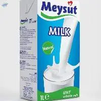
1. Product: UHT MILK 2. Description UHT Milk is obtained from raw milk, normalized to determined contents of fat, and then treated a sterilization process UHT and aseptic packaging. 3. Technical requirements 3.1. Packaging and transport â?? direct packaging of UHT Milk is a carton which is made of multilayer laminate with Aluminum foil of a capacity 1 litter. A direct packaging are placed on cardboard palettes. 3.2. Labelling A direct packaging of UHT milk is marked with: Name and address of the producer, Name of product, Type of heat treatment: UHT Expire date : ,,Best before:â??- day, month, year, storage conditions Fat content, Net weight, 3.3 Nutritional value in 100 ml: 4. STORAGE UHT milk should be stored in dry, clean, warehouse, no longer than 9 months from production date, at temperature below +25�°C. After opening the carton should be stored under refrigerated conditions and no longer than 48 hours. Payment : TT
Gold plated multi layered pendant chain necklace Chain: Choker Clasp: Lobster Collection: Latest Multilayer Western Neckpiece Neck Chain Stone: No Gemstone Material: Metal Metal: Alloy
LAYER FPCB S/S Application Medical equipment Thickness 0.06T L/S 50/50 LASER CUT tolerance +-50 Surface treatment SILVER Inspection spec Zero defect SPECIAL item for controlling Film coating and resolution Will apply scale for Laser individual recognition
Multilayer Tarpaulin are the best and reasonable product for agriculture purpose and others. It's Available in 90 GSM only. Blue and yellow colour available.
Brand Name: HK CT TECH OEM PCB Model Number: Double sided,Multilayer pcb Base Material: FR4,Rogers,Aluminum Copper Thickness: 0.1oz-8oz pcb circuit board Board Thickness: 0.2mm-4mm Min. Hole Size: 0.1mm-1mm Surface Finishing:HASL,LEAD FREE HASL,OSP Product name: Shenzhen prototype design service pcb circuit board PCB type :Customized Electronics Manufacturing Optional laminate Material: Alu/Aluminum,FR4/FR-4,Copper,Ceramic,Rogers Solder mask color: Blue,Red,Purple,Yellow,White,Green,Black Number of Layer: 2 layer,8 layer,multi-layer PCBB Certification of quantum board led: ISO/UL/TS16949/RoHS/TS16949 PCB Standards: IPC-A-610 D/IPC-III Standard Service: PCBA,PCB&PCBA Design&Clone&Production Application: Consumer Electronics,Industrial,Electronical Products,Battery Pack PCB Assembly service: SMT THT DIP
8 layer 1mm HDI PCB 0 gap 8 layer PCB, 0 gap PCB, 1mm PCB 1) Thickness: 0.1mm-5mm 2) Minimum linewidthï¼?0.075mm/3mil 3) Minimum gapï¼?0.065/2.8mil 4) Minimum aperture inradiumï¼?0.15mm 5) Minimum aperture external diameterï¼?0.45mm 6) Minimum BGA: 0.2mm 7) Layerï¼?4 layers through hole non-impedance All multilayer boards are printed with 36t screen, the resistance welding oil is 50 tons thicker than the traditional 43t, which provides reliability guarantee for the bga and more precise fine lines.
Specification: Layer count: 4 Laminate: FR4 PCB Thickness: 1.6mm PCB size: 480mm X 420 mm Finished copper: 1oz/1oz/1oz/1oz Soldermask color: Green Silkscreen color: White Surface finish: ENIG Outline: CNC Routing Min Lind width/ space: 5mil/4mil Test: 100%
Dear Friend, If you find this PCB product, maybe you know that PCB is customized product. So above unit price is not real. Details pls feel free contact me, and quotation will be arranged for you. Thank you very much for all your support. : ) Best regards, Andwin 1 Layer to 52 Layer Printed Circuit Board for Electronic Products could meet all your PCB manufacturing needs,including High multilayer PCB, Aluminum based PCB, HDI PCB, Rigid-flex PCB, heavy copper PCB, and PCB assembly as well. Our products are widely applied in telecom, industrial control, power electronics, medical instrument , security electronics, aerospace and so on.And Provides "PCB One-stop PCB solution" to meet customers' diverse demands. PCB board manufacture and PCB assembly service: -PCB board file with parts list provided by customers - PCB board made, circuit board parts purchased by us - High Quality,competitive Price & Best Service -100% E-test Testing Procedures For PCB Board: ----We perform multiple quality assuring procedures before shipping out any PCB board. These include: - Visual Inspection - Flying probe - Impedance control - Solder ability detection - Digital metallogenic microscope - AOI (Automated Optical Inspection) Quotation Requirement : ----Following specifications are needed for quotation: -Quantity -Base material -Board thickness -Copper thickness -Surface treatment -Color of solder mask and silkscreen Notice: Please send me your PCB files in gerber files by email to sales8#andwinpcb.com Delivery Lead Time for PCB board: -Quickturn for sample : 2 layers 24 Hours, 4 layers 2 days or 3 days. -General sample: 3 - 5days. -Mass production: within 7 days. Shipping Method and Payment terms: -By DHL, UPS, FedEx, TNT using clients account. -DHL, UPS, FedEx, TNT forwarder of China. -According to package weight ,we will tell you the freight. -Shipping the parcel by Russia Special Air Line for Russian customer (Notice: No TAX in your there, 3-10 days to Moscow, 15-20 days to other city) -By sea or air for mass quantity according to customer's requirement. -By customer's Forwarder -Payment By Paypal, T/T, West Union, etc.
Key specifications/special features: specifications: Base material: fr4, pcb, Layer count: 4 layer board Board thickness: 1.6mm Copper thickness: 1oz Surface finishing: immersion gold Soldermask color: green Available specifications: Base materials: fr4, aluminum, fpc and copper Copper thickness: 0.5oz (minimum) Copper thickness: 4oz (minimum) Board thickness: 0.2mm (minimum) Board thickness: 3.2mm (maximum) Surface finishing: hal, enig, osp, gold finger and tin chemistry Possible soldermask colors: green, black, white, yellow, blue, red and more Board dimensions: 600 x 1, 000mm Hole diameter: 0.2mm (minimum) Line width: 0.075mm (minimum)
Multilayer standard up to 18 layers Fr-1/2, cem-1/3, fr-4, high tg fr-4 Copper thickness: 0.5-3 oz Board thickness: 0.4-3.2mm Tracks and gaps standard >= 0.1mm Surface finish: osp, hasl(leaded or unleaded), immersion tin/silver/gold, plate gold Ball grid arrays
Bicheng provides RD, high-tech, IT research companies and organizations, large and small with multi-layer PCB's. It covers: 1) 4-32 Layers, 0.5-6mm thick 2) High Tg 170, High CTI 600V 3) Impedance control +/-10% 4) 1+C+1 HDI, Buried/blind vias 5) Half hole, Via in pad, countersink hole 6) ENIG, HASL, Immersion Silver, OSP, Gold finger, peelable mask 7) Rogers and FR-4 combination PCB. 8) BGA, CSP, QFN 9) Quick turn prototype 10) Small and volume production. Vaccum bags.
1. Rigid PCB boards 2. Attained UL ,ISO,CQC certificate 3. IPC Class 2 standard 4. 8-9 working days for printed circuit board. Inner : vacuum packing/plastic bag Outer : standard carton packing.
Track width/ space: 8mils/8mils Hole diameters: 0.3mm Copper Weight: 1/1/1/1oz Solder Mask: Green Surface Treating: HASL.
1~16Layer Material CEM-3,FR-4, High TG, Halogenfree, Rogers, BT(Bismalemide Triazine) Free Finish Board Thicknes 0.2mm~3.20mm(8mil~126mil) Copper Thickness 1/2 OZ min 3 OZ max Min. Trace Width & line Spacing 0.075mm¡ê¡§3mil¡ê© Flash gold Min. Hole Diameter CNC Drilling 0.33mm(12mil) 0.25mm(10mil).
Surface finish : lead free hasl, immersion gold, gold plating osp immersion pin Min line width: 3mil Min line space: 3mil Min space between pad to pad :3 mil Min hold diameter 0.1um Max size of finish board: 23inch*35inch Max proportion drilling hold and bord thickness: 1:12.5 Rang of finish board thickness: 0.21~0.7mil Min tickness soldermask :10um Min line width of idents: 4mil Min height of idents: 25mil Color of silk screen: yellow white blue Soldermask: green yellow blue red balck white transparent photesensitive soldermask strippable soldermask Date file foemat: gerber file, drilling file, protel series , pads2000series, powerpcb series odb++ E test: 100% e test, high voltage test Material pcb: fr4 high tg fr4 halogen free, rogers, cem-1 , arlon taconic, ptfe, isola.
Material: fr-4 Board finish thickness 1.6mm Product size: 294mm*215mm Min line width: 5mil Min line spacing: 5mil Min hole size: 0.3mm Surface treament: osp Vacuum packing/plastic bag