Material: fr-4 tg180 Board thickness: 2.0mm Min line/space: 0.127/0.127mm Min hole size: 0.25mm Surface treatment: immersion gold

we are leading manufacturer & exporter of standoff/spacers as per requirement or Drawing
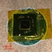
We just processed in a large batch of chipsets. I posted below current inventory and attached pictures of each type of chipset. Please review and let me know your interest/offer. Chipset 1 (H61) â?? 3,350 units Chipset 2 (H81) â?? 2,206 units Chipset 3 (H55) â?? 436 units Chipset 4 (B250) â?? 1,600 units Chipset 5 (SR406) â?? 345 units Thank you, Divanti Group
Double side to 24 layer PCB, blinded and buried hole board.
Layer printed circuit boards rigid, rigid flex, back planes, high frequency board, controlled impedance bga blind/buried via pcbs.
Multilayer PCB (2-18 layers) aluminum PCB, blind, buried via and HDI and heavy copper PCB.
Layer count:20l Base material: fr-4 tg170 Copper thickness: all layers 2oz Board thickness: 3.2mm±0.3mm Min hole diameter: 0.50mm(19mil) Min trace width: 0.20mm(8mil) Min trace spacing: 0.20mm(8mil) Suface finishing: enig Test: flying probe Panel dimension: 106.63mmx134.42 mm Panel method: 6up, 2*3 Blind:dr1-2, dr3-4, 2 step blind vias Via diameter: 0.5mm(19mil) Lead time:fastest 10wds, normal 15-20 wds
6L, BGA-Multilayer PCB 6 Layer PCB Board, BGA PCB, Multilayer PCB, Special Technology PCB, Metal Core PCB, High-Level HDI Hole Technology, Blind Buried Hole PCB, Impedance Control PCB Supplier Layer/Board thickness: 6L/1.6mm Suface Finish: ENIG Trace/Space: 5/6mil Smallest Hole Diameter: 0.2MM PCBMAIN provides special technology PCB with high-level HDI hole technology such as metal core PCB, blind buried hole PCB, impedance control PCB, BGA PCB and multilayer PCB such as 6 layer PCB board, 4 layer PCB board, , 8 layer PCB board, 10 layer PCB board, 12 layer PCB board.
Dear Friend, If you find this PCB product, maybe you know that PCB is customized product. So above unit price is not real. Details pls feel free contact me, and quotation will be arranged for you. Thank you very much for all your support. : ) Best regards, Andwin 1 Layer to 52 Layer Printed Circuit Board for Electronic Products could meet all your PCB manufacturing needs,including High multilayer PCB, Aluminum based PCB, HDI PCB, Rigid-flex PCB, heavy copper PCB, and PCB assembly as well. Our products are widely applied in telecom, industrial control, power electronics, medical instrument , security electronics, aerospace and so on.And Provides "PCB One-stop PCB solution" to meet customers' diverse demands. PCB board manufacture and PCB assembly service: -PCB board file with parts list provided by customers - PCB board made, circuit board parts purchased by us - High Quality,competitive Price & Best Service -100% E-test Testing Procedures For PCB Board: ----We perform multiple quality assuring procedures before shipping out any PCB board. These include: - Visual Inspection - Flying probe - Impedance control - Solder ability detection - Digital metallogenic microscope - AOI (Automated Optical Inspection) Quotation Requirement : ----Following specifications are needed for quotation: -Quantity -Base material -Board thickness -Copper thickness -Surface treatment -Color of solder mask and silkscreen Notice: Please send me your PCB files in gerber files by email to sales8#andwinpcb.com Delivery Lead Time for PCB board: -Quickturn for sample : 2 layers 24 Hours, 4 layers 2 days or 3 days. -General sample: 3 - 5days. -Mass production: within 7 days. Shipping Method and Payment terms: -By DHL, UPS, FedEx, TNT using clients account. -DHL, UPS, FedEx, TNT forwarder of China. -According to package weight ,we will tell you the freight. -Shipping the parcel by Russia Special Air Line for Russian customer (Notice: No TAX in your there, 3-10 days to Moscow, 15-20 days to other city) -By sea or air for mass quantity according to customer's requirement. -By customer's Forwarder -Payment By Paypal, T/T, West Union, etc.
Characteristic Capability Production Capacity 800,000 sq.ft/Month Layer(mass production) 1 to 24 Layers Max Panel Size 450*660mm Base Copper Thickness 1/3 OZ --5 OZ Impedance Control +/-8% Board ThicknessImpedance Control Min:6mil(0.15mm) Max:280mil(7mm) Blind/Buried hole YES Drilling (Minimum size) Mechanical drilling 8mil(0.2mm) Laser drilling 4mil(0.1mm) Inner Etching Minimum line/Space(A/W) 2.5mil(0.0625mm) Line Width Tolerance +/-8% Board Thickness(min) 2.5mil(0.625mm) Plating Hole Minimum Hole Size 6mil (0.15mm) Aspect Ratio (max) 12:01 Position Accuracy +/-1.8mil(0.045mm) Microvia Minimum Hole Size 3mil(0.075mm) Aspect Ratio (max) 1:01 Outer Etching Minimum Width /Space 2.5mil(0.05mm) Line Width Tolerance +/-0.4mil(0.01mm) Solder Mask Bridge 3.0mil(0.075mm) Position Accuracy 1.5mil(0.0375mm) Selective Gold Plating Gold Thickness 100u ís (2.5um) Press Thickness Tolerance 8% Wrap/Twist 0.70% Inner Opening (min) (1) 4/L:5mil(0.125mm) (2) 6/L-8/L:6mil(0.15mm) (3) 8/L or above:8mil(0.2mm) Lead Time sample S/D L:3days;4-8L:5-15days mass productioníí S/D L:5days;4-8L:10-25days Base Material Special Technology Surface Finish CEM-1/CEM-3/FR-4 FR4(Halogen free) High-speed & high-frequency material High Tg/CTI material Al-base PTFE,Rogers,Getek,BT,Polyimide blind hole PCB buried resistor PCB laser-drill HDI PCB mix-material PCB Plating edge PCB buried via PCB impedance control PCB heavy Cu PCB (5oz) Counter-Sink PCB ; HASL &Lead Free HASL Chem. Ni/Au Chem. Tin Ni/Au plating Flash Gold Gold finger OSP &F2 Chem. Silver
Quotation requirement : ----following specifications are needed for quotation: -quantity -base material -board thickness -copper thickness -surface treatment -color of solder mask and silkscreen Notice: please send me your pcb files in gerber files by email to sales8#andwinpcb.Com 1 layer to 52 layer printed circuit board for electronic products could meet all your pcb manufacturing needs, including high multilayer pcb, aluminum based pcb, hdi pcb, rigid-flex pcb, heavy copper pcb, and pcb assembly as well. Our products are widely applied in telecom, industrial control, power electronics, medical instrument , security electronics, aerospace and so on.And provides "pcb one-stop pcb solution" to meet customers’ diverse demands.
Dear Friend, If you find this PCB product, maybe you know that PCB is customized product. So above unit price is not real. Details pls feel free contact me, and quotation will be arranged for you. Thank you very much for all your support. : ) Best regards, Andwin 1 Layer to 52 Layer Printed Circuit Board for Electronic Products could meet all your PCB manufacturing needs,including High multilayer PCB, Aluminum based PCB, HDI PCB, Rigid-flex PCB, heavy copper PCB, and PCB assembly as well. Our products are widely applied in telecom, industrial control, power electronics, medical instrument , security electronics, aerospace and so on.And Provides "PCB One-stop PCB solution" to meet customers' diverse demands. PCB board manufacture and PCB assembly service: -PCB board file with parts list provided by customers - PCB board made, circuit board parts purchased by us - High Quality,competitive Price & Best Service -100% E-test Testing Procedures For PCB Board: ----We perform multiple quality assuring procedures before shipping out any PCB board. These include: - Visual Inspection - Flying probe - Impedance control - Solder ability detection - Digital metallogenic microscope - AOI (Automated Optical Inspection) Quotation Requirement : ----Following specifications are needed for quotation: -Quantity -Base material -Board thickness -Copper thickness -Surface treatment -Color of solder mask and silkscreen Notice: Please send me your PCB files in gerber files by email to sales8#andwinpcb.com Delivery Lead Time for PCB board: -Quickturn for sample : 2 layers 24 Hours, 4 layers 2 days or 3 days. -General sample: 3 - 5days. -Mass production: within 7 days. Shipping Method and Payment terms: -By DHL, UPS, FedEx, TNT using clients account. -DHL, UPS, FedEx, TNT forwarder of China. -According to package weight ,we will tell you the freight. -Shipping the parcel by Russia Special Air Line for Russian customer (Notice: No TAX in your there, 3-10 days to Moscow, 15-20 days to other city) -By sea or air for mass quantity according to customer's requirement. -By customer's Forwarder -Payment By Paypal, T/T, West Union, etc.
Fr4 standard pcb from 2 ~ 28 layer Fpcb, rigid-flex pcb from 1 ~ 12 layer Metal substrates pcb (al / cu based pcb) High tg , halogen free, heavy copper pcb High frequency, mixed delectric pcb (teflon material) Hdi pcb, blind and buried via board, impedance control pcbs
PCB Scope: Heavy Copper PCB, Hard Gold PCB, Bridge Connecting Leiterplatte, Blind & Buried �¼ber PCB, Bleifreie Leiterplatte, Halogenfreie Leiterplatte, High Frequency / TG / Density PCB, Gold Ginger PCB, OSP, Flash Gold PCB, FPC, Flex -Platte
Dear Friend, If you find this PCB product, maybe you know that PCB is customized product. So above unit price is not real. Details pls feel free contact me, and quotation will be arranged for you. Thank you very much for all your support. : ) Best regards, Andwin 1 Layer to 52 Layer Printed Circuit Board for Electronic Products could meet all your PCB manufacturing needs,including High multilayer PCB, Aluminum based PCB, HDI PCB, Rigid-flex PCB, heavy copper PCB, and PCB assembly as well. Our products are widely applied in telecom, industrial control, power electronics, medical instrument , security electronics, aerospace and so on.And Provides "PCB One-stop PCB solution" to meet customers’ diverse demands. PCB board manufacture and PCB assembly service: -PCB board file with parts list provided by customers - PCB board made, circuit board parts purchased by us - High Quality,competitive Price & Best Service -100% E-test Testing Procedures For PCB Board: ----We perform multiple quality assuring procedures before shipping out any PCB board. These include: - Visual Inspection - Flying probe - Impedance control - Solder ability detection - Digital metallogenic microscope - AOI (Automated Optical Inspection) Quotation Requirement : ----Following specifications are needed for quotation: -Quantity -Base material -Board thickness -Copper thickness -Surface treatment -Color of solder mask and silkscreen Notice: Please send me your PCB files in gerber files by email to sales8#andwinpcb.com Delivery Lead Time for PCB board: -Quickturn for sample : 2 layers 24 Hours, 4 layers 2 days or 3 days. -General sample: 3 - 5days. -Mass production: within 7 days. Shipping Method and Payment terms: -By DHL, UPS, FedEx, TNT using clients account. -DHL, UPS, FedEx, TNT forwarder of China. -According to package weight ,we will tell you the freight. -Shipping the parcel by Russia Special Air Line for Russian customer (Notice: No TAX in your there, 3-10 days to Moscow, 15-20 days to other city) -By sea or air for mass quantity according to customer's requirement. -By customer's Forwarder -Payment By Paypal, T/T, West Union, etc.
1 layer to 52 layer printed circuit board for electronic products could meet all your pcb manufacturing needs, including high multilayer pcb, aluminum based pcb, hdi pcb, rigid-flex pcb, heavy copper pcb, and pcb assembly as well. Our products are widely applied in telecom, industrial control, power electronics, medical instrument , security electronics, aerospace and so on.And provides "pcb one-stop pcb solution" to meet customers’ diverse demands. Quotation requirement : ----following specifications are needed for quotation: -quantity -base material -board thickness -copper thickness -surface treatment -color of solder mask and silkscreen
Dear Friend, If you find this PCB product, maybe you know that PCB is customized product. So above unit price is not real. Details pls feel free contact me, and quotation will be arranged for you. Thank you very much for all your support. : ) Best regards, Andwin 1 Layer to 52 Layer Printed Circuit Board for Electronic Products could meet all your PCB manufacturing needs,including High multilayer PCB, Aluminum based PCB, HDI PCB, Rigid-flex PCB, heavy copper PCB, and PCB assembly as well. Our products are widely applied in telecom, industrial control, power electronics, medical instrument , security electronics, aerospace and so on.And Provides "PCB One-stop PCB solution" to meet customers’ diverse demands. PCB board manufacture and PCB assembly service: -PCB board file with parts list provided by customers - PCB board made, circuit board parts purchased by us - High Quality,competitive Price & Best Service -100% E-test Testing Procedures For PCB Board: ----We perform multiple quality assuring procedures before shipping out any PCB board. These include: - Visual Inspection - Flying probe - Impedance control - Solder ability detection - Digital metallogenic microscope - AOI (Automated Optical Inspection) Quotation Requirement : ----Following specifications are needed for quotation: -Quantity -Base material -Board thickness -Copper thickness -Surface treatment -Color of solder mask and silkscreen Notice: Please send me your PCB files in gerber files by email to sales8#andwinpcb.com Delivery Lead Time for PCB board: -Quickturn for sample : 2 layers 24 Hours, 4 layers 2 days or 3 days. -General sample: 3 - 5days. -Mass production: within 7 days. Shipping Method and Payment terms: -By DHL, UPS, FedEx, TNT using clients account. -DHL, UPS, FedEx, TNT forwarder of China. -According to package weight ,we will tell you the freight. -Shipping the parcel by Russia Special Air Line for Russian customer (Notice: No TAX in your there, 3-10 days to Moscow, 15-20 days to other city) -By sea or air for mass quantity according to customer's requirement. -By customer's Forwarder -Payment By Paypal, T/T, West Union, etc. PCB Prototype Lead Time: item General time Quick Turn 1-2 4 days 1 days 4-6 Layers 6 days 2 days 8-10 Layers 8 days 3 days 12-16 Layers 12 days 4days 18-20 Layers 14 days 5 days 22-26 Layers 16 days 6 days Note: Base on all data received by us and must be complete and problem free,Lead time is ready to ship time.
1 Layer to 52 Layer Printed Circuit Board for Electronic Products could meet all your PCB manufacturing needs,including High multilayer PCB, Aluminum based PCB, HDI PCB, Rigid-flex PCB, heavy copper PCB, and PCB assembly as well. Our products are widely applied in telecom, industrial control, power electronics, medical instrument , security electronics, aerospace and so on.And Provides "PCB One-stop PCB solution" to meet customers’ diverse demands. PCB board manufacture and PCB assembly service: -PCB board file with parts list provided by customers - PCB board made, circuit board parts purchased by us - High Quality,competitive Price & Best Service -100% E-test Testing Procedures For PCB Board: ----We perform multiple quality assuring procedures before shipping out any PCB board. These include: - Visual Inspection - Flying probe - Impedance control - Solder ability detection - Digital metallogenic microscope - AOI (Automated Optical Inspection) Quotation Requirement : ----Following specifications are needed for quotation: -Quantity -Base material -Board thickness -Copper thickness -Surface treatment -Color of solder mask and silkscreen Notice: Please send me your PCB files in gerber files by email to sales8#andwinpcb.com Delivery Lead Time for PCB board: -Quickturn for sample : 2 layers 24 Hours, 4 layers 2 days or 3 days. -General sample: 3 - 5days. -Mass production: within 7 days. Shipping Method and Payment terms: -By DHL, UPS, FedEx, TNT using clients account. -DHL, UPS, FedEx, TNT forwarder of China. -According to package weight ,we will tell you the freight. -Shipping the parcel by Russia Special Air Line for Russian customer (Notice: No TAX in your there, 3-10 days to Moscow, 15-20 days to other city) -By sea or air for mass quantity according to customer's requirement. -By customer's Forwarder -Payment By Paypal, T/T, West Union, etc.
Dear Friend, If you find this PCB product, maybe you know that PCB is customized product. So above unit price is not real. Details pls feel free contact me, and quotation will be arranged for you. Thank you very much for all your support. : ) Best regards, Andwin 1 Layer to 52 Layer Printed Circuit Board for Electronic Products could meet all your PCB manufacturing needs,including High multilayer PCB, Aluminum based PCB, HDI PCB, Rigid-flex PCB, heavy copper PCB, and PCB assembly as well. Our products are widely applied in telecom, industrial control, power electronics, medical instrument , security electronics, aerospace and so on.And Provides "PCB One-stop PCB solution" to meet customers' diverse demands. PCB board manufacture and PCB assembly service: -PCB board file with parts list provided by customers - PCB board made, circuit board parts purchased by us - High Quality,competitive Price & Best Service -100% E-test Testing Procedures For PCB Board: ----We perform multiple quality assuring procedures before shipping out any PCB board. These include: - Visual Inspection - Flying probe - Impedance control - Solder ability detection - Digital metallogenic microscope - AOI (Automated Optical Inspection) Quotation Requirement : ----Following specifications are needed for quotation: -Quantity -Base material -Board thickness -Copper thickness -Surface treatment -Color of solder mask and silkscreen Notice: Please send me your PCB files in gerber files by email to sales8#andwinpcb.com Delivery Lead Time for PCB board: -Quickturn for sample : 2 layers 24 Hours, 4 layers 2 days or 3 days. -General sample: 3 - 5days. -Mass production: within 7 days. Shipping Method and Payment terms: -By DHL, UPS, FedEx, TNT using clients account. -DHL, UPS, FedEx, TNT forwarder of China. -According to package weight ,we will tell you the freight. -Shipping the parcel by Russia Special Air Line for Russian customer (Notice: No TAX in your there, 3-10 days to Moscow, 15-20 days to other city) -By sea or air for mass quantity according to customer's requirement. -By customer's Forwarder -Payment By Paypal, T/T, West Union, etc.
Multiplayer thick copper PCB, high frequency mixing plate, 18-layer multiplayer PCB, multiplayer thick copper PCB, HDI buried & blind via PCB, aluminum base, high frequency copper plate, LED board.