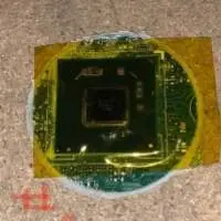
Please click here to check who's online and chat with them.

4 Layer Osp Circuit Board

Supplier From China
Oct-11-11

Layer count: 4
Surface treatmeat: osp
Soldermask color: green
Silkscreen color: yellow
Final board thickness: 1.60mm.
Minimum line width/space: 0.10/0.12mm.
Minimum via hole: 0.30mm.

Price and Minimum Quantity

Price: $5
MOQ: Not Specified

Recent User Reviews

This user has not received any reviews yet!

Verification Status


Contact Supplier
Renew

More Items Similiar to: 4 Layer Osp Circuit Board

GOLD Member
May-13-20
Supplier From Garfield Heights, Ohio, United States
 
We just processed in a large batch of chipsets. I posted below current inventory and attached pictures of each type of chipset. Please review and let me know your interest/offer.

Chipset 1 (H61) â?? 3,350 units
Chipset 2 (H81) â?? 2,206 units
Chipset 3 (H55) â?? 436 units
Chipset 4 (B250) â?? 1,600 units
Chipset 5 (SR406) â?? 345 units


Thank you,

Divanti Group
GOLD Member
Nov-27-24
Supplier From Shenzhen, China
Aug-21-19
Supplier From Shenzhen, Shenzhen, China
 
Gold OSP 6 layers mobile phone circuit board
Gold OSP circuit board
1) Thickness: 0.1mm-5mm
2) Minimum linewidthï¼?0.075mm/3mil
3) Minimum gapï¼?0.065/2.8mil
4) Minimum aperture inradiumï¼?0.15mm
5) Minimum aperture external diameterï¼?0.45mm
6) Minimum BGA: 0.2mm
7) Layerï¼?6 layers through hole non-impedance 
All multilayer boards are printed with 36t screen, the resistance welding oil is 50 tons thicker than the traditional 43t, which provides reliability guarantee for the bga and more precise fine lines.
Feb-13-20

Osp Printed Circuit Board

$1
MOQ: Not Specified
Supplier From Shenzhen, Shenzhen, China
 
green solder mask PCB, OSP printed circuit board
1) Thickness: 0.1mm-5mm
2) Minimum linewidth 0.075mm/3mil
3) Minimum gap 0.065/2.8mil
4) Minimum aperture inradium 0.15mm
5) Minimum aperture external diameter 0.45mm
6) Minimum BGA: 0.2mm
7) Layer 4 layers through hole non-impedance 
All multilayer boards are printed with 36t screen, the resistance welding oil is 50 tons thicker than the traditional 43t, which provides reliability guarantee for the bga and more precise fine lines.
GOLD Member
Dec-15-23
Supplier From Dubai, United Arab Emirates
Dec-16-15
Supplier From Huizhou, Guangdong Province, China
 
4 layer board, blud soldermask, immersion gold surface finishing.


Depend on customer requirements.
Dec-02-15
Supplier From Shenzhen, China
 
2 layers rigid-flex pcb
Minimum line width/space: 8mils
Surface finish: immersion gold
Board thickness: 0.50mm
Minimum drilled hole diameter: 8mils
Copper thickness: 0.5oz
Special process : 0.10mm flexible pcb inside


Carton
GOLD Member
VERIFIED
Mar-08-25

Inp Wafers, WAFERS

$350 - $2.50K / Piece (CIF)
MOQ: 10  Pieces
Sample Available
Supplier From South Hackensack, New Jersey, United States
 
INDIUM PHOSPHIDE (InP) WAFERS are semiconductor materials made of indium phosphide, a compound semiconductor that is widely used in high-frequency and optoelectronic applications. Due to its efficient electron mobility and direct bandgap properties, InP is favored for devices such as:

High-speed electronics
Laser diodes
Photodetectors
Telecommunications applications, including optical fiber communication
We offer the following InP Wafers:
Undoped InP Wafers: These are pure InP with no intentional doping, used in various applications where intrinsic properties are required.
N-type InP Wafers: Doped with donor impurities (such as tellurium) to increase electron concentration, useful in transistors and high-speed electronics.
P-type InP Wafers: Doped with acceptor impurities (such as zinc) to create holes in the semiconductor, used in light-emitting devices and other optoelectronics.
InP Substrates: Used as a base for growing other semiconductor materials in heterostructures for various applications.
InP Membrane Wafers: Thin layers of InP used for specific applications, including applications in flexible electronics and advanced photonic devices.
InP-based Quantum Dot Wafers: Engineered to create quantum dots that can be used in photonic and optoelectronic devices for enhanced performance.
Dec-06-22
 
Flexible printed circuit boards are used to make interconnections in systems that have no room for rigid PC boards. Flex circuits are bendable and lightweight and are used in applications where the circuit is bent or flexed in two or more planes in the assembly or installation process.

Verification Status