We just processed in a large batch of chipsets. I posted below current inventory and attached pictures of each type of chipset. Please review and let me know your interest/offer.
Chipset 1 (H61) â?? 3,350 units
Chipset 2 (H81) â?? 2,206 units
Chipset 3 (H55) â?? 436 units
Chipset 4 (B250) â?? 1,600 units
Chipset 5 (SR406) â?? 345 units
All weather traction
Enhanced controllability
Fuel efficient drive
Excellent durability
The Hankook Smart Flex AH35 is a highway terrain all-season tire manufactured for commercial vehicles. The tyre model is made to be mounted on the vehicle's steering axle.
Hankook Smart Flex AH35 - Key Features
All-Weather Performance: The tire offers reliable traction in dry, wet, and winter conditions, thanks to its wide grooves and 3D sipes, which also prevent hydroplaning.
Enhanced Control: The ribbed tread design ensures constant road contact, improving steering response and driving stability.
Fuel Efficiency: The optimized 3D siping reduces rolling resistance, leading to lower fuel consumption and CO2 emissions.
Durability: Reinforced carcass structure maintains the tire's shape under heavy loads, extending tread life and making it cost-efficient.
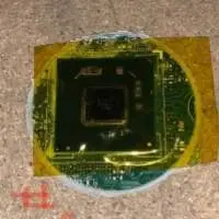
IC Chips, IC, Recycle, Reuse or Repair
These IC Chips are for reuse or for recovery of minerals, gold, silver and more.
All ICs are mixed with fingers, no finders.
These are ready for shipping, sold in small quantity or in bulk.
Please feel free to contact our resale agent for more information.
Price is price on request and quantity, please contact for more information.
Our Product Range
4-28 layer of high-precision impedance, blind & buried layers, HDI boards, high frequency board,
halogen-free boards, high-TG boards, aluminum, copper, iron base and ceramic-based circuit board,
1-6 layer flexible circuit board ( FPC) and rigid-flex flexible board, and other high-tech products.
PCB Process Capability
processing layers: 1- 30 layers
Finished thickness: 0.008 "~ 0.24" (0.20mm ~ 6.0mm)
Minimum aperture: 6mil (0.15mm)
Minimum line width / spacing: 3-4 mil (0.076-0.10mm)
Maximum board size: Single & Double 22 "x 43" (550 x1100mm), Multi-layer 22 "x 25" (550mm x 640mm)
Impedance Control: ± 10%
Surface Treatment: OSP, HASL, Electric Nickel / Gold, Chemical nickel / gold, lead-free HASL , Gold finger,
immersion Silver, Immersion Tin.
Base materials: FR4 ( ShengYi, KB, International), high TG (TG150, TG170), halogen-free board (Halogen-free),
High frequency plate (Rogers, Teflon, Taconic), made PTFE (PTFE), AL aluminum plate (Berquist, Al-made basis),
copper (Cu Base), Iron (Fe Base), Ceramic substrate (Ceramic Base)
INDIUM PHOSPHIDE (InP) WAFERS are semiconductor materials made of indium phosphide, a compound semiconductor that is widely used in high-frequency and optoelectronic applications. Due to its efficient electron mobility and direct bandgap properties, InP is favored for devices such as:
High-speed electronics
Laser diodes
Photodetectors
Telecommunications applications, including optical fiber communication
We offer the following InP Wafers:
Undoped InP Wafers: These are pure InP with no intentional doping, used in various applications where intrinsic properties are required.
N-type InP Wafers: Doped with donor impurities (such as tellurium) to increase electron concentration, useful in transistors and high-speed electronics.
P-type InP Wafers: Doped with acceptor impurities (such as zinc) to create holes in the semiconductor, used in light-emitting devices and other optoelectronics.
InP Substrates: Used as a base for growing other semiconductor materials in heterostructures for various applications.
InP Membrane Wafers: Thin layers of InP used for specific applications, including applications in flexible electronics and advanced photonic devices.
InP-based Quantum Dot Wafers: Engineered to create quantum dots that can be used in photonic and optoelectronic devices for enhanced performance.