we are leading manufacturer & exporter of standoff/spacers as per requirement or Drawing
We just processed in a large batch of chipsets. I posted below current inventory and attached pictures of each type of chipset. Please review and let me know your interest/offer. Chipset 1 (H61) â?? 3,350 units Chipset 2 (H81) â?? 2,206 units Chipset 3 (H55) â?? 436 units Chipset 4 (B250) â?? 1,600 units Chipset 5 (SR406) â?? 345 units Thank you, Divanti Group
Hankook Smart Flex AH35 FEATURES AND BENEFITS All weather traction Enhanced controllability Fuel efficient drive Excellent durability The Hankook Smart Flex AH35 is a highway terrain all-season tire manufactured for commercial vehicles. The tyre model is made to be mounted on the vehicle's steering axle. Hankook Smart Flex AH35 - Key Features All-Weather Performance: The tire offers reliable traction in dry, wet, and winter conditions, thanks to its wide grooves and 3D sipes, which also prevent hydroplaning. Enhanced Control: The ribbed tread design ensures constant road contact, improving steering response and driving stability. Fuel Efficiency: The optimized 3D siping reduces rolling resistance, leading to lower fuel consumption and CO2 emissions. Durability: Reinforced carcass structure maintains the tire's shape under heavy loads, extending tread life and making it cost-efficient.
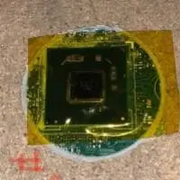
Brand Name: strongtimes Number of Layers: 4 Base Material: FR-4 Copper Thickness: 3mil Board Thickness: 1.6mm Min. Hole Size: 4mil Min. Line Width: 3mil Min. Line Spacing: 3mil Surface Finishing: lead free hal Printed Circuit board, Single Side PCB, Double Side PCB, Multilayer PCB, Rigid Flexible PCB, Rigid PCB, Flexible PCB, Impedance PCB, HDI PCB, MCPCB, FPC, Aluminum PCB, PCB, PCBA StrongTimes Electronics Co., Ltd is a high and new technological company which specializing in manufacturing single-sided, double-sided and multilayer PCB of high precision, high density and high reliability.
Specializing in Double Side PCB, Multi-Layer PCB, F4BK PCB, Ceramic PCB, Rogers PCB, Aluminum PCB. Meanwhile, we provide PCBA ( Assembly) and ODM, OEM service. We are specializes in a full SMT and through hole PCBA assembly, obtaining components, building prototype quantities, and testing. Layer: 1- 4 Layers Material: Rogers2000-6000 Board Thickness: 0.4-2.0 mm Copper thickness: 0.5- 2OZ Treatment : Lead Free HASL, ENIG, Immersion Tin, Immersion Silver, OSP ,Gold palting etc. Solder Mask : Green, Red, White, Yellow, Black, Blue, or NO soldering mask; * We can provide quick turn prototype and small quantity PCBs with short lead time. * The quality of Our products is excellent and stable. * We choose the best material for all our products. * We will send the boards to you by DHL, TNT, UPS, FEDEX and so on to saving the transport time. * For responding promptly, we will reply your e-mail from 9: 00am to 23: 00pm by two shifts. We sincerely hope to establish longtime and friendly business relationship with you. Good quality, reasonable price and the 5-Star service are guaranteed.
Dear Friends, Our company specializes in producing High Mix & Medium-small series Rigid PCBs(1-28layers),Rigid-flex pcbs as well as AL pcbs in China . As a Sales Manager in my company, I have worked in PCB industry over than 10year since my graduation from University . We exported a lot of PCBs to Europe and America countries for several years . I expect to know more parnters all over the world through here.
Jinsung Electronics company produces High-end Rigid-Flex PCB which is used for multiple product groups such as smartphones, camera module, electric apparatuses, medical devices, defense articles, and so on supplying to domestic and global market 1. LAYER : 6 Layer (FLEXIBLE 2 layer+RIGID 4 layer) 6-2-6 2. Application : Inspection equipment of Semiconductor 3. Thickness : 0.5T 4. Structure : 1-2LBVH ,2-3L BVH 1-4 STACK BVH , 4-6BVH , 56BVH 5. Machine Drill : Min. 0.25mm 6. Cu Plating : VIA FILL + PTH 7. BGA(LAND/PTICH) : 0.3 mm / 0.4pitch
What is HDI PCB High density interconnect (HDI) PCB, represent one of the fastest growing technologies in PCBs. Because of its higher circuitry density than traditional circuit boards, the HDI PCB design is able to incorporate smaller vias and capture pads, and higher connection pad densities. HDI Boards contain blind and buried vias and often contain micro vias of 0.006 or less in diameter. By using HDI technology, designers now have the ability to place more components on both sides of the raw PCB if desired. Now as the development of via in pad and blind via technology, it allow designers to place smaller components closer together. This means faster transmission of signals and a significant reduction in signal loss and crossing delays. HDI PCB is regularly found in mobile phones, touch-screen devices, laptop computers, digital cameras, 4G network communications, also prominently featured in medical devices. Advantages of HDI PCB The most common reason for using HDI technology is a significant increase in packaging density. The space that obtained by finer track structures is available for components. In addition, overall space requirements are reduced will result in smaller board sizes and fewer layers. Usually FPGA or BGA are available with 1mm or less spacing. HDI technology makes routing and connection easy, especially when routing between pins.
General specification for hdi pcb Layer count: 4-20layers Type of stack up: 1+n+1, 2+n+2 Material available: fr4, high tg fr4, halogen free fr4 Board thickness: 0.4-3.2mm Finished copper thickness: 1/3oz ¡§c 3oz Min trace width/spacing: 3/3mil Min through hole: 0.2mm Min blind via: 0.1mm Surface treatment: immersion gold, enig + osp Vacuum package